
Low Leakage Switch Matrix
RM1010-LLC
Low Leakage Relay Matrix Mainframe
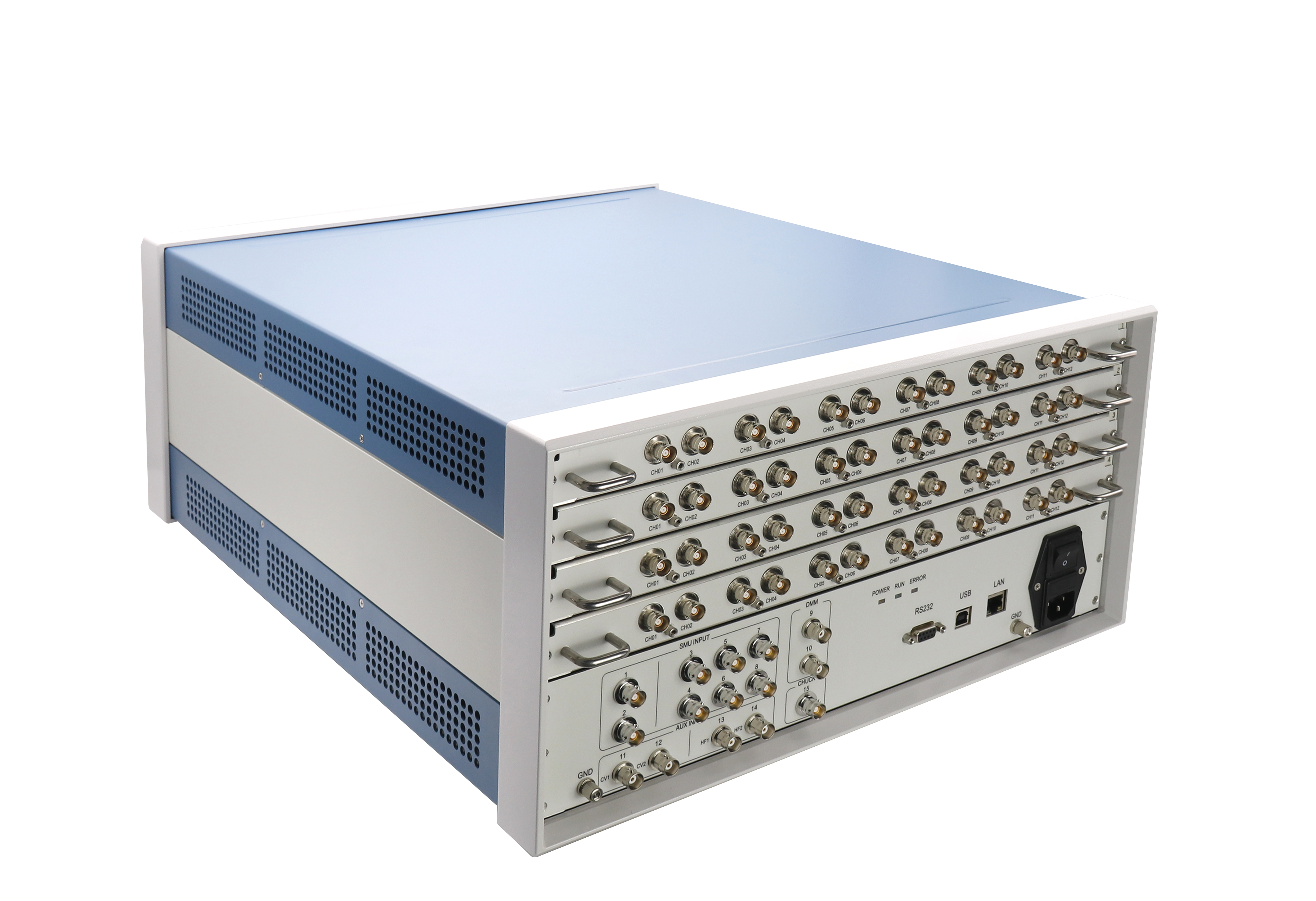
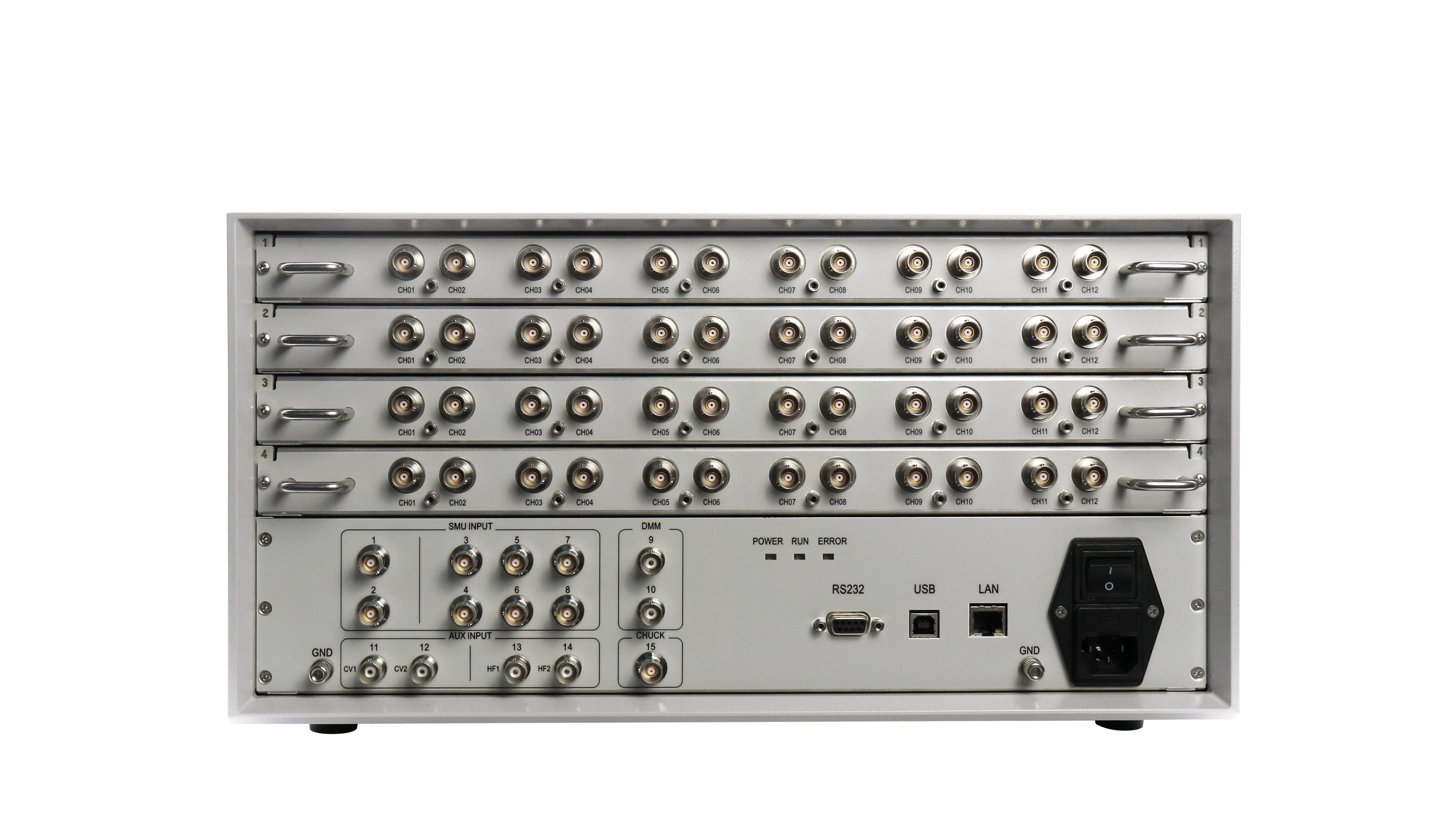
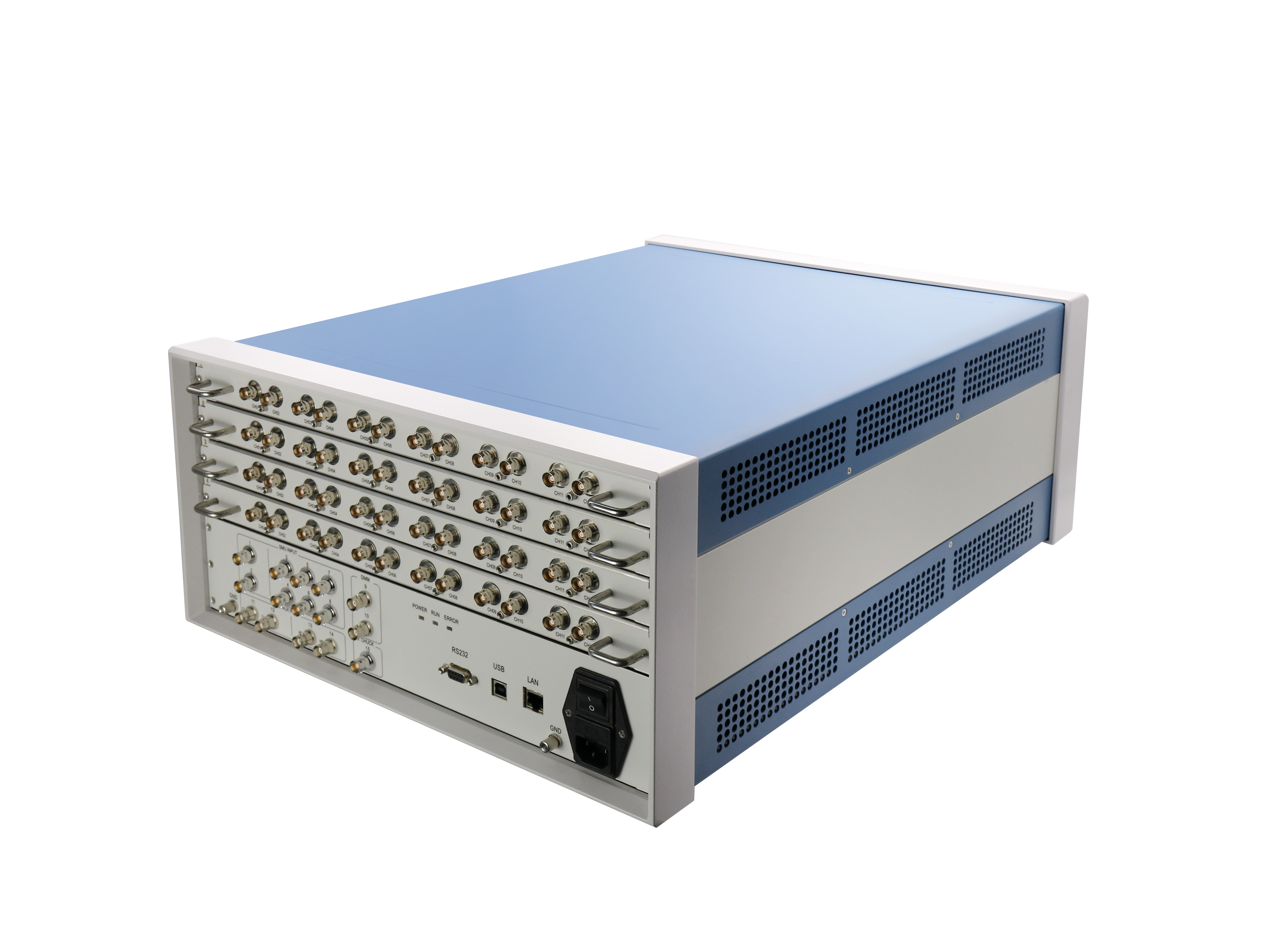
RM1010-LLC is a 4-slot semiconductor switch matrix that can meet high-speed semiconductor test applications by integrating S3022F benchtop or S2012C PXle SMU. Easy-to-use GUI helps to speed up the development of new test functions and simplify system integration. It supports traditional SCPI commands, enabling easy and fast programming of test code. It can support multi-machine parallel connection to achieve test efficiency improvement and cost reduction.
Features

Multi-channel Flexible Measurement
Supports for 2-channel low leakage current input
Low Leakage Current
The minimum achievable leakage current <100 fA
Rapid Measurement
The establishment time of weak current <3.5s
High Relay Contact Life
The switch life >10^8 times
10MHz BW
Optimize the transmission bandwidth of C-V and HF channels
Supports 2 Control Methods
Run the upper computer GUI software on the PCFunctions and Advantages
Precise, Consistent Results
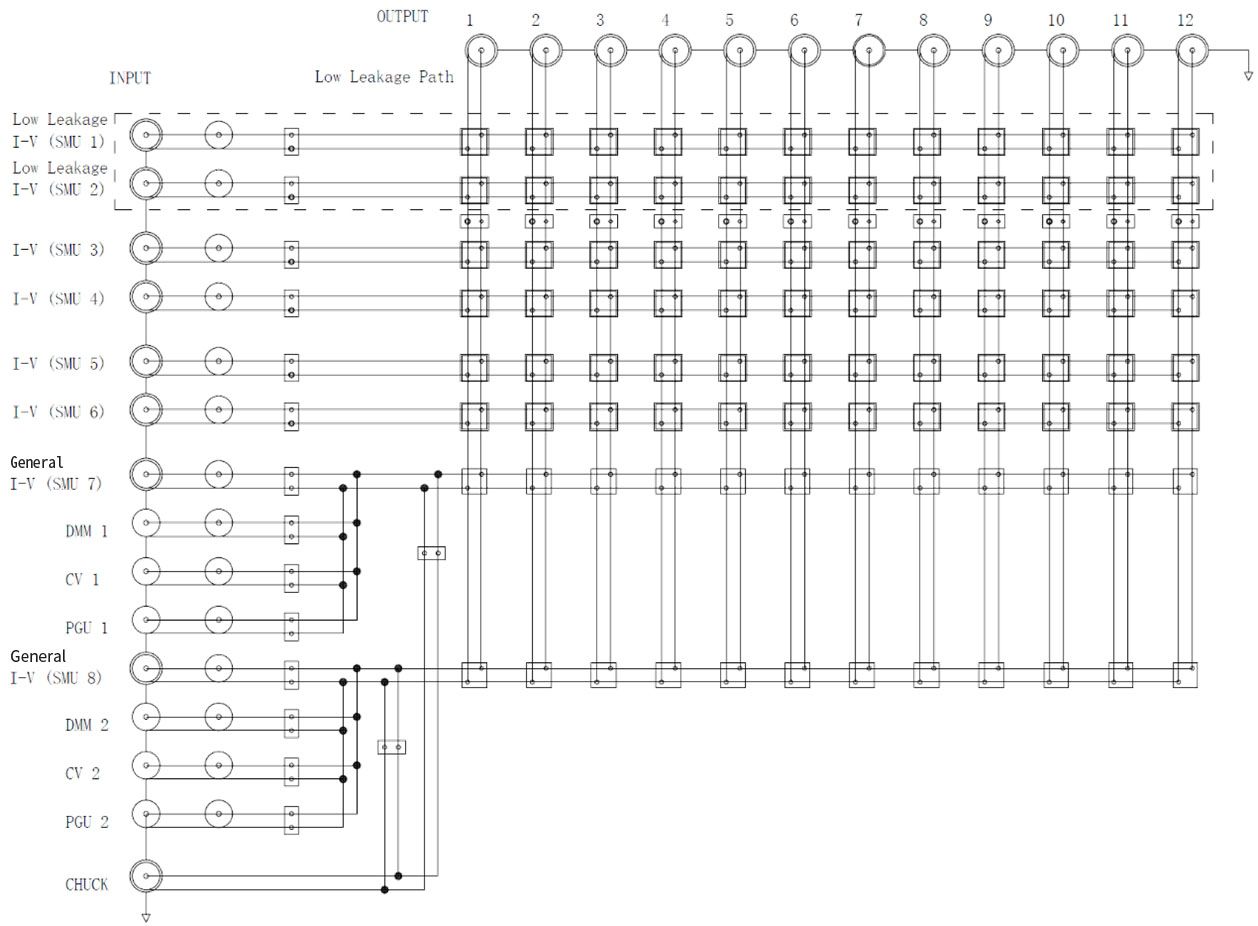
Supports 2 channels of low leakage current input, the whole machine supports 14 inputs and 48 outputs.
|
Specification |
|
2(Low Leakage I-V Port) 6(General I-V Port) 2(C-V Port) 2(DMM Port) 2(PGU Port) |
| Ouput Channels | 12/24/36/48 | |
| Max. Current Rating | 1 A | |
| Max. Voltage Rating |
200V(Channel to Ground) 300V (Channel to Channel) |
|
|
|
0.6 Ω(Low Leakage I-V Port) 1.0 Ω(General I-V Port) 1.0 Ω(C-V, HF Port) |
|
|
|
1013 Ω(Low Leakage I-V Port) 1012 Ω(General I-V Port) 109 Ω(C-V, HF Port) |
|
|
Typical Data |
Offset Current | <100fA(Low Leakage I-V Port) <1000pA(General I-V Port) |
|
|
<80μV(Low Leakage I-V Port) <110μV(General I-V Port) <110μV(C-V, HF Port) |
|
| Channel Crosstalk Capacitance | <0.3pF/CH |
Similar recommendation

High speed communication test plays an important role in the rapid development of big data, cloud computing, 5G communication and other markets.
Semight offers various of instruments for optical Transceiver/Component testing, including wide bandwidth sampling oscilloscope, NRZ/PAM4 bit error ratio tester , burst error ratio tester, fast wavelength meter, high precise source measure unit, 400G network analyzer ,optical power meter, optical attenuator, optical switch etc. We provide cost-effective, complete solutions for optical testing.

The high-precision source measure units integrates the functions of voltage source, current source, voltmeter, ampere meter, and electronic load in one, which is widely used in high-precision IV test and measurement for various discrete components, photovoltaic, green energy, battery and other industries. Semight provides high-precision benchtop SMU and plug-in PXIe SMU of standard PXIe chassis, fully meeting the application of various test scenarios.
Details
Burn-in testing of laser is an important method to ensure the reliability of laser. Through the test of CoC or bare die, the early failure of laser caused by the defects in the process of laser production can be screened out in advance. Semight provides a complete solution from bare die to CoC, from high temperature(150℃ or higher) to low temperature (-40℃), with CoC automatic loading and unloading system, forming a complete test solution, Semight's laser chip burn-in/load/unload test system has been widely recognized by the market.
Details
The semiconductor front-end test is mainly used in the wafer processing to check whether the processing parameters of the wafer products meet the design requirements or there are defects affecting the yield after each step of the manufacturing process. The semiconductor back-end test equipment is mainly used after wafer processing to check whether the performance of the chip meets the requirements, which belongs to the electrical performance test. Semight provides solutions such as Wafer Level Burn In system and Known Good Die handler for SiC testing, offering the value to customer in test efficiency improvement and test cost reduction.
DetailsFollow
Name
E-mail verfication code
Phone
Password
Confirm Password
E-mail address
E-mail verification code
New Password
Confirm Password
 Ask for demo