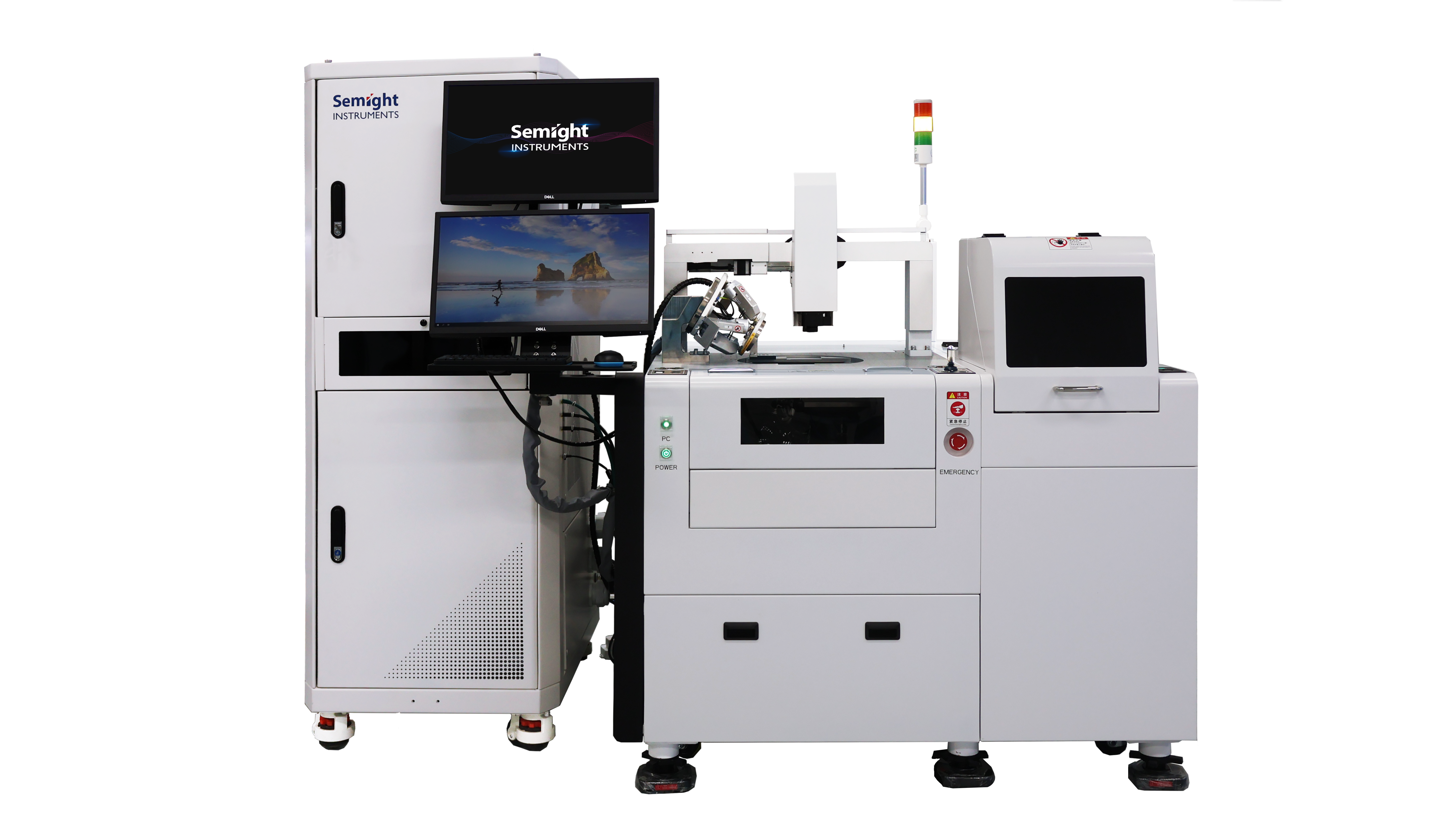
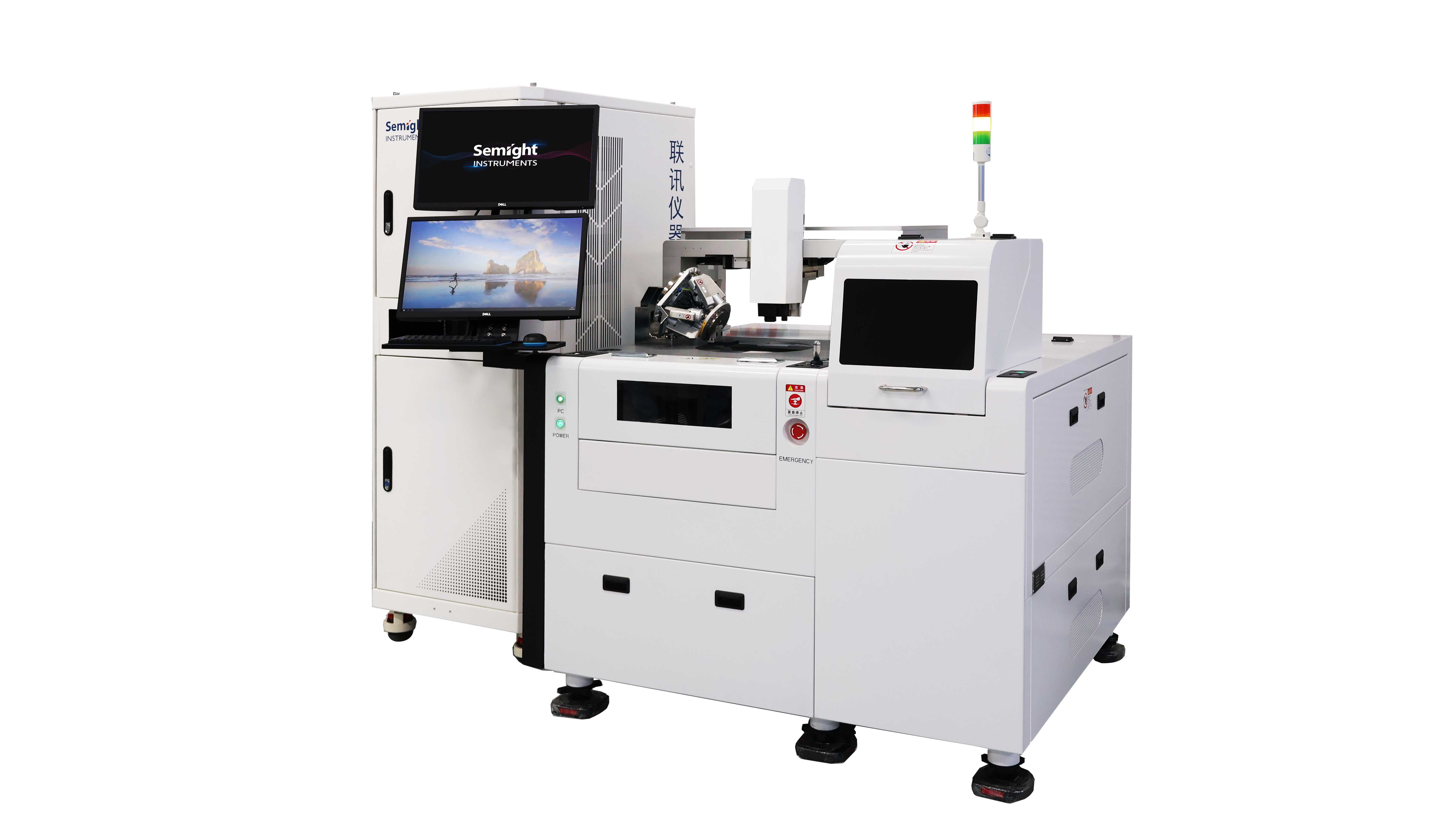
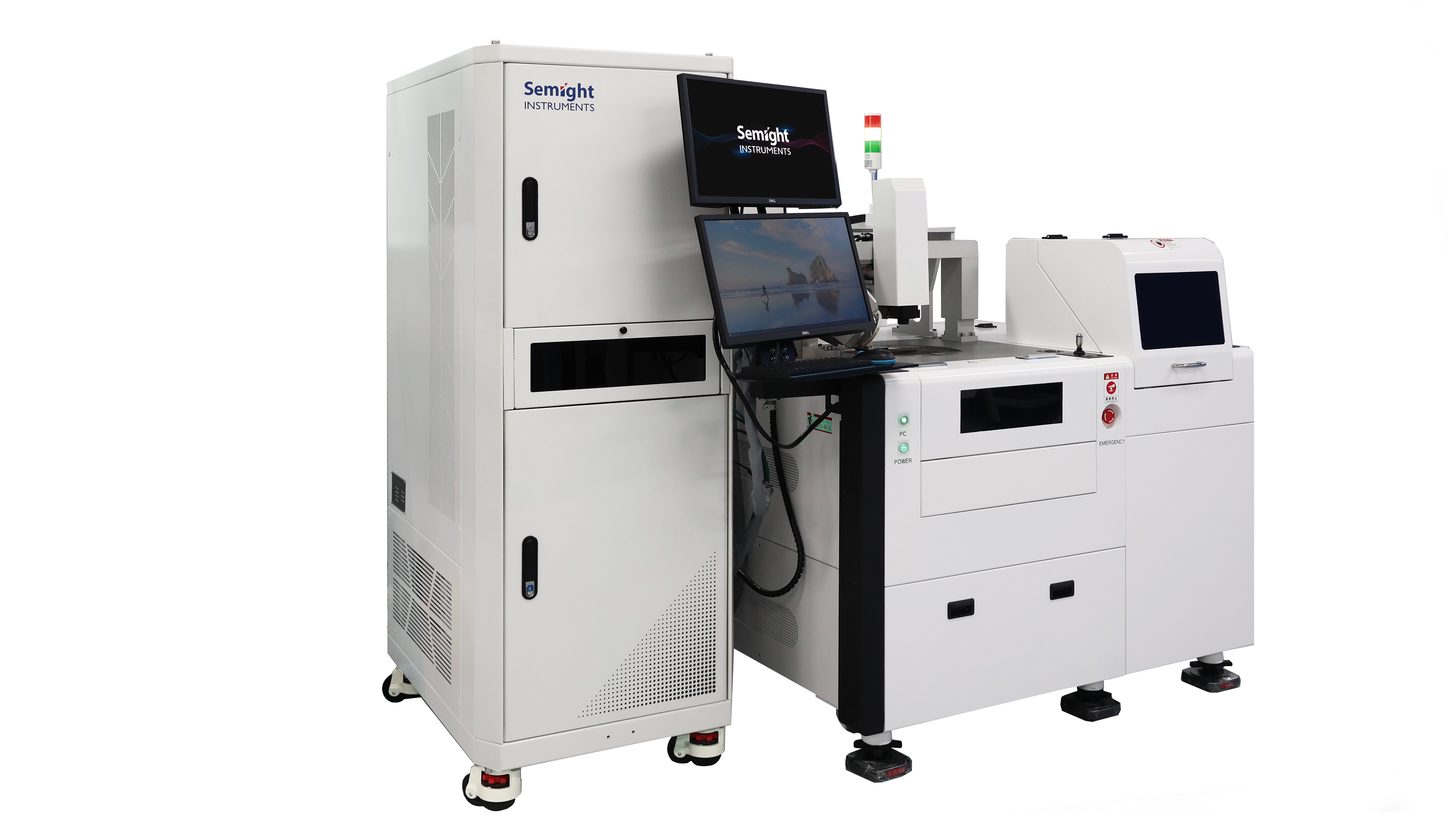

Silicon Photonics
sCT9001
SiPh Wafer Test System
Features

Automatic/Semi-automatic
Supports automatic and semi-automatic wafer loading and unloading
Wafer Size
Supports 8-inch and 6-inch wafers
Test Temperature
Supports the test temperature range from room temperature to 150 ℃ (other temperatures can be customized)
Test Function
Supports optical-optical test, photoelectric test and electrical parameter test
DC/AC
Supports DC and AC test
Grating Vertical Coupling
Grating coupling, FA coupling, and edge coupling
High Efficiency
For different types of chips, supports rapid replacement of different types of pin cards
Software Function
The software supports the addition of customer database and MES functionsFunctions and Avantages
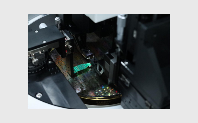
High Accuracy Probe Station
Wafer loading mode supports fully automatic mode and semi-automatic mode operation, which is suitable for laboratory verification and mass production.
The fully closed-loop high-accuracy motion control system is provided with automatic accuracy compensation function and its positioning accuracy is up to 3μm.
The special mechanism design and calibration system can make the wafer on chuck have better planarity and better perpendicularity in Z direction of probe.
A high-definition zooming CCD configured on the system can make the power on PAD clearly visible and display low-magnification and high-magnification multi-view screens at the same time.
The built-in integrated shock-proof design is adopted which can isolate the external vibration and ensure a good test stability.
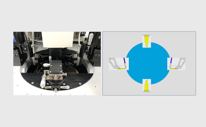
Coupling Test Module
The coupling test module includes coupling optical probe, DC probe and RF probe.
The optical probe supports single-channel coupling and dual-channel coupling.
The optical probe is provided with a high-precision altimeter to ensure the consistency of the height from the incident fiber end face to the chip surface between different chips.
The optical fiber coupling module is composed of a three-dimensional lead screw motor matched with a three-dimensional high-precision piezoelectric ceramic module to ensure the optical coupling efficiency and the optical coupling repeatability.
The standard high-precision coupling controller configured on the system which can help the system realize the functions of fully closed-loop control and hardware synchronization improve the coupling accuracy and coupling speed.
The design of the probe card holder is more convenient for the replacement of the probe card, which is convenient to quickly replace the probe card for different products or different test items.
|
CHUCK |
Platform |
Material |
Cast iron |
|
Chuck X&Y Axis |
Motor type |
Servo motor |
|
|
Travel range X*Y |
≥240 mm * 340 mm |
||
|
Resolution |
0.1 μm |
||
|
Positioning accuracy |
±2 μm |
||
|
Max speed |
200 mm/s |
||
|
Chuck Z Axis |
Motor type |
Stepper motor |
|
|
Travel range |
≥30 mm |
||
|
Resolution |
0.2 μm |
||
|
Positioning accuracy |
±2 μm |
||
|
Max speed |
30 mm/s |
||
|
Chuck θ Axis |
Motor type |
Stepper motor |
|
|
Travel range |
±8° |
||
|
Resolution |
0.001° |
|
Coupled Module |
Motion and positioning |
Hexapods + Piezo |
6 serial axis +Piezo |
|
Max number of active axes |
9 |
9 |
|
|
Rotation for roll, yaw and pitch |
Automated |
Automated |
|
|
Stepping for X, Y, Z |
Automated |
Automated |
|
|
Rough Positioning |
|||
|
Travel range X,Y,Z |
±17, ±15, ±7 mm |
±15, ±15, ±10 mm |
|
|
Travel range θX, θY, θZ |
±9, ±8.5, ±18° |
±6, ±5, ±6° |
|
|
Minimum incremental motion X, Y, Z |
±0.10, ±0.10, ±0.05 μm |
±0.10, ±0.10, ±0.10 μm |
|
|
Minimum incremental motion θx, θy, θz |
0.05mdeg, 0.05mdeg, 0.1mdeg |
0.01deg, 0.01deg, 0.01deg |
|
|
Fine Positioning |
|||
|
Travel range in X, Y, Z, closed loop |
80 μm |
||
|
Min. incremental motion, open-loop |
0.4 nm |
||
|
Min. incremental motion, closed-loop |
4 nm |
||
|
Alignment Speed |
|||
|
Scanning time of spiraled area scan |
<1.5 s |
||
|
Note |
For vertical coupling only, purchasing the 8-axis system is sufficient. To be compatible with both vertical and edge coupling, the 9-axis system is required |
||
|
Coupling Specification |
Optical coupling speed |
<1.5s @ unilateral coupling |
|
Coupling repeatability |
<0.2 dB (30 times) |
|
|
Optical power stability |
<0.2 dB@5 min |
Similar recommendation

High speed communication test plays an important role in the rapid development of big data, cloud computing, 5G communication and other markets.
Semight offers various of instruments for optical Transceiver/Component testing, including wide bandwidth sampling oscilloscope, NRZ/PAM4 bit error ratio tester , burst error ratio tester, fast wavelength meter, high precise source measure unit, 400G network analyzer ,optical power meter, optical attenuator, optical switch etc. We provide cost-effective, complete solutions for optical testing.

The high-precision source measure units integrates the functions of voltage source, current source, voltmeter, ampere meter, and electronic load in one, which is widely used in high-precision IV test and measurement for various discrete components, photovoltaic, green energy, battery and other industries. Semight provides high-precision benchtop SMU and plug-in PXIe SMU of standard PXIe chassis, fully meeting the application of various test scenarios.
Details
Burn-in testing of laser is an important method to ensure the reliability of laser. Through the test of CoC or bare die, the early failure of laser caused by the defects in the process of laser production can be screened out in advance. Semight provides a complete solution from bare die to CoC, from high temperature(150℃ or higher) to low temperature (-40℃), with CoC automatic loading and unloading system, forming a complete test solution, Semight's laser chip burn-in/load/unload test system has been widely recognized by the market.
Details
The semiconductor front-end test is mainly used in the wafer processing to check whether the processing parameters of the wafer products meet the design requirements or there are defects affecting the yield after each step of the manufacturing process. The semiconductor back-end test equipment is mainly used after wafer processing to check whether the performance of the chip meets the requirements, which belongs to the electrical performance test. Semight provides solutions such as Wafer Level Burn In system and Known Good Die handler for SiC testing, offering the value to customer in test efficiency improvement and test cost reduction.
DetailsFollow
Name
E-mail verfication code
Phone
Password
Confirm Password
E-mail address
E-mail verification code
New Password
Confirm Password
 Datasheet
 Ask for demo